
|
Hytec Electronics Ltd. |

|
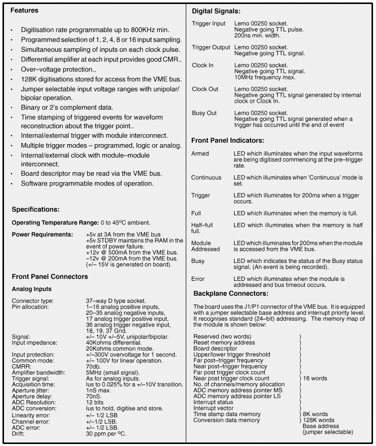
VME VTD 1612 Transient Digitiser Product Description The Transient Digitiser is a dual height single width VME slave board which provides the digitisation and storage of analog waveforms present on up to sixteen differential input channels. Each input is provided with a track/hold circuit so that all channels can be simultaneously sampled. The sampled voltages are multiplexed into a fast 12–bit ADC which has its own sample/hold amplifier. The ADC digitises the voltage and stores the resultant binary information in a 128K word RAM. Memory can be allocated according to the number of inputs selected, ie: 1, 2, 4, 8, or 16 inputs use 128K, 64K, 32K, 16K or 8K words per input. The RAM is dual–ported and provides access for both the ADC and VME bus. The board has programmable operating modes. Its main modes are: Triggered Buffer Mode Three clock frequencies can be selected for pre–trigger, near post–trigger and far post–trigger digitisation rates. Memory is equally divided between the pre–trigger and post–trigger buffers. When the module is armed by software command, clocking occurs at the pre–trigger frequency in the pre–trigger buffer. A trigger causes digitisation to occur at the near post–trigger frequency for a specified number of samples from the start of the post–trigger buffer followed by the far post–trigger frequency for a second specified number of samples. On completion, acquisition is halted. Continuous Mode Normally, when the ’Full flag’ interrupts, digitisation is inhibited. However, it is possible to set up a continuous mode wherein digitisation occurs continuously. The ’Half full’ and ’Full’ flags can then be used as an indication of where in memory digitisation has reached, so that alternate halves of memory can be read whilst still acquiring data. Samples are clocked at the pre–trigger clock frequency and the whole memory is used as a pre–trigger buffer. Single Scan Mode In this mode the pre–trigger clock is inhibited. When the VTD is triggered the input voltages are sampled and converted, the memory address pointer is incremented, and the ’end of event’ interrupt status bit is set. it is possible to trigger multiple scans using post–trigger counts of greater than one.
The board can interrupt for one or all of three states:– It is possible to read the contents of an addressed memory location via the VME bus whilst the board is digitising. This concurrent access mode is permitted once per ADC conversion, ie: not exceeding a read rate of one megaword per second. At the trigger point the current memory address will be recorded in a time–stamp buffer. Up to 8192 time stamps can be recorded. The board can be triggered from an external analog source, from channel 1, by an external logic pulse, or by software command. The clock frequency can be programmed from 1MHz down to 0.01Hz using either an internal or external clock source with a maximum frequency of 8MHz. The clock is buffered and is transmitted via a front panel connector. Provision is made for connecting Clock Out to Clock In of another module. Trigger is also buffered and transmitted as a logic pulse via a connector so that one module can trigger another. |
| Hytec Electronics Ltd Post : 5 Cradock Road, Reading, Berkshire, RG2 0JT, England. Phone : +44 (0)118 9757770 Fax : +44 (0)118 9757566 |