
Hytec Electronics Ltd
VVA4032
VME-VXI Adapter
General Description
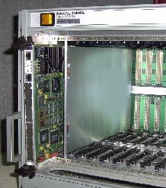
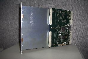
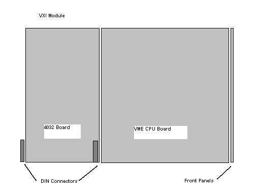
The VVA4032 is a C sized VXI module which extends and buffers the
VME subset of the VXIbus to a pair of DIN 96 way connectors suitable for
accepting a B size VME processor card. It includes a VME slave interface
which provides the VXI configuration registers, controls for the MODID lines
and access to the other sub-units of the 4032 system.
The slave control logic is implemented using a Xilinx FPGA device with boot
PROM. This gives the ability to change the slave configuration registers with
ease.
Those configuration
registers which are not currently defined and some which are reserved are
implemented as RAM giving the ability to software test the slave on power-up.
The buffering of the VME bus includes those lines whose direction of drive
cannot be predicted. The bi-directional drivers are implemented using part of
the Xilinx FPGA and high current buffers with open collector outputs.
Software Interface
The VME slave in the adapter module is accessed in the short I/O region of the VME address space. It is an A16/D16 slave with interrupter capability. Since it forms the configuration registers for the VXI slot 0 function it has a fixed address of V=0. The configuration register space is a part of the VME short I/O address space. The address is calculated from V*40h+C000h where V is the logical address. This leads to an address of @C000h for this slave.
The address space occupies 64 bytes. The function of some of the
words is defined in the VME specification; others are user definable. The
Resource Manager requires the implementation of a message based device in the
crate with location monitors on specific configuration register accesses. The
necessary signalling to the processor is carried out via a VME interrupt. The
configuration registers and the device dependent registers and their bit
functions are shown below:
|
Address |
Function |
Contents |
|
0 |
ID ( R ) |
ID number etc. |
|
2 |
Device type ( R ) |
Mdel code etc |
|
4 |
CSR S ( R ) C ( W ) |
Control & status bits |
|
6 |
A24/A32 offset ( R/W ) |
Not used |
|
8 |
Protocol ( R ) Signal ( W ) |
Indicates protocolsFor device-device signals |
|
A |
Response ( R ) Data extended ( W ) |
Communication status |
|
C |
Data high ( R/W ) |
Data reg with loc monitor |
|
E |
Data low ( R/W ) |
Data reg with loc monitor |
|
10-1E |
Reserved ( R/W ) |
Implemented as RAM |
|
20 |
MODID ( R/W ) |
Bits 12-0 MODID Bit 13 enable |
|
22 |
Location monitor Status ( R ) / control ( W ) |
Bits 7-0 Intr vector |
|
24 |
External
bus address (W) |
15-0
ext address |
|
26 |
Externa
data word ( R/W ) |
15-0
ext data |
|
28-2E |
RAM
( R/W ) |
15-0 |
|
30-36 |
Not
used |
|
|
38 |
Signal
( R ) / Protocol ( W) |
|
|
3A |
Response(W)/
Ext data (R |
Processor
access |
|
3C |
Data
high ( R/W ) |
Processor
access |
|
3E |
Data
low ( R/W ) |
Processor
access |
Layout (6 unit wide version)
For
information on Hytec products and services please contact:
|
HYTEC Head
Post : 5 Cradock Road, Reading, Berkshire, RG2 0JT, England. |
Copyright © 2002 [Hytec Electronics
Ltd]. All rights reserved.
Information in this document is subject to change without notice.
Other products and companies referred to herein are trademarks or registered
trademarks of their respective companies or mark holders.
Last modified: October 29, 2008